In the previous article on reading digital input, we learned how to use the PORT and ANSEL registers to read from a digital input device. However, I didn’t explain how we knew that those were the registers to read from. In this tutorial, we’ll dive into the microcontroller’s datasheet — the 500-page monstrosity that details everything we could possibly want to know about our MCU’s internals — and learn how to find out about analog inputs for ourselves.
Diving into the datasheet
Let’s start by opening up the datasheet. Go to the Digikey page for the PIC16F15345, scroll down a little bit, and click on “
PIC16(L)F15325/45 Datasheet” to pull it up.
Don’t be intimidated by the mass of technical details in front of you — we don’t need to read all of it! We’ll go section by section and learn how to find the info we need. Microchip, the company that makes PIC micros, uses a similar format for most of their microcontrollers, so once we get familiar with it, we’ll be able to work with any of them.
The first important bit we need to look at is the title in the top-right corner, which is easily overlooked. We’re using the PIC16F15345 model, but this datasheet also covers the PIC16F15325 (as well as the PIC16LF15325/45 models, which are low-voltage variants). Make a note of this, as some of the later tables and charts in the datasheet reference one of those particular models — and it may not be the one we’re using! This is a mistake lots of microcontroller newbies make, so always remember to check the model number. We’ll see some examples of this shortly.
The next few pages describe the features and highlights of the models in the datasheet, which is great information if you’re selecting a MCU to use in a project. We’ve already selected ours, so we’ll scroll past this to page 5, “Pin Diagrams”. Here we see diagrams showing pinouts for the different microcontrollers. Many ICs come in multiple different packages — the type of chip. The PIC16F15345, comes in both the 20-pin DIP package that we’re using and a 20-pin QFN package, which is used for custom circuit boards. Also note that some of the pin diagrams are for the 15345 and some are for the 15325, so look for the correct one.
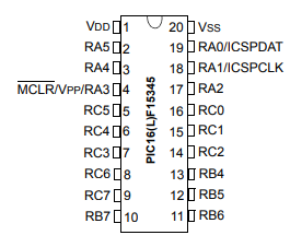
This pin diagram tells us what’s on what pin, which you’ll need to know when you’re designing your own microcontroller circuits. Of particular importance are the power pins (VDD/VSS) and the programming pins (MCLR, ICSPDAT and ICSPCLK), which are sometimes listed instead as PGD and PGC. Many other PIC models also have CLKIN and CLKOUT pins labeled on the pin diagram, which are where we’d connect a crystal oscillator if we wanted to use one.
Let’s scroll down a bit more. On page 7 we have the “Pin Allocation Tables”, which describe the peripheral modules available on each pin. Look at the top of the table: it’s for the 14/16-pin PIC16(L)F15325, which means this is the wrong table! Further down we have another table for the 20-pin PIC16(L)F15345, which is the one we want. Don’t worry too much about this table yet, we’ll come back to it later.
Next we have the table of contents on page 11. Looking through it, we see that there is a chapter for each of the peripherals. For example, if we wanted to know more about the GPIO ports we’ve been using so far, we would go to chapter 14, “I/O Ports”. The TOC also lists chapters with general information, such as a “Device Overview” and “Guidelines for Getting Started with PIC16(L)F15325/45 Microcontrollers”. Take a look if you’re interested. Right now we want to start reading analog inputs, so click on chapter 20, “Analog-to-Digital Converter (ADC) Module” to jump to that chapter.
The ADC peripheral
Every chapter about a peripheral starts with a section describing the functions for that peripheral. I’d highly recommend you try and read through the first few pages of the ADC description; don’t worry if some of it doesn’t make sense. Let’s look at the first paragraph:
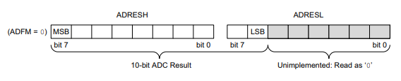
The Analog-to-Digital Converter (ADC) allows conversion of an analog input signal to a 10-bit binary representation of that signal. This device uses analog inputs, which are multiplexed into a single sample and hold circuit. The output of the sample and hold is connected to the input of the converter. The converter generates a 10-bit binary result via successive approximation and stores the conversion result into the ADC result registers (ADRESH:ADRESL register pair).
What is this saying? The ADC converts an analog voltage into a numerical value. The ADC is 10 bit, which means that the numerical value is 10 bits long. So, for example, if the pin we’re reading the analog voltage from has 0V on it, the numerical value we’ll read is 0b0000000000, or 0 in decimal. If the pin has 5V, we’ll read 0b1111111111, or 1023. Any voltage in between 0V and 5V will be converted to a number that’s proportionally scaled between 0 and 1023 (for example, 1V will be converted to a value of 1023/5 = 205, or 0b0011001101). Thus, we can write code that reads this number and converts it to the correct input voltage. In general, if we read a value x, we know that the voltage input to our ADC is (x/1023) * 5V.
The description also mentions that the ADC result is stored in two different registers: ADRESH and ADRESL (ADC Result High/Low registers). Why? Because we’re using a 8-bit microcontroller! Every register is 8 bits, which means a 10-bit value must be stored in two separate registers. By default, ADRESH stores the upper 8 bits of the conversion result and ADRESL’s upper 2 bits are used for the 2 low bits of the conversion result; this is described in the “Result Formatting” section (20.1.6).
Now let’s get to the meat of the problem: how do we know which registers to use, and what to do with them? Scrolling down to page 230 (section 20.2.6), we see a step-by-step explanation of how to configure and use the ADC module. This is good stuff, but we’ll skip it for just a minute. Keep going, and let’s take a look at page 233: Section 20.4, “Register Definitions”.
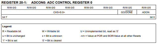
This is the answer to all of our questions: the register definition tables tell us how to access each peripheral in the microcontroller. Above the table, we see that we’re looking at the ADCON0 register (ADC control register 0). Below that, we see that the register (8 bits in total) is split into several bitfields: bit 0 is the ADON bit, bit 1 is the GO/DONE bit, and bits 2 through 7 comprise the CHS bitfield.
Right below the table we see a description of each bit. For instance, we see that setting ADON to 1 enables the ADC module, which tells us that somewhere in our code we’ll have:
ADCON0bits.ADON = 0b1;
We also see that setting the GO/DONE bit starts a new ADC conversion, and that this bit is automatically cleared in hardware when the conversion is done. So we’ll do something like:
ADCON0bits.GOnDONE = 0b1;
while(ADCON0bits.GOnDONE);	//wait until the bit is automatically cleared
				//in the IDE, if you type "ADCON0bits.", a dropdown with the struct bitfield names will pop up
//do the conversion
The CHS bitfield allows us to set the ADC channel we’ll be reading from. This is separate from enabling a pin’s ADC functionality with the ANSEL register — just because a pin’s ANSEL bit is set doesn’t mean that pin is the selected channel. We’re reading from pin RC6, so we can set that as the ADC pin with:
ADCON0bits.CHS = 0b010110;
The next register table, for register ADCON1, has a few more bitfields for setting more ADC paramters. For now we only care about one of these: the ADC conversion clock (ADCS) bits. From reading the description at the beginning of the chapter, we know that this determines how long the ADC module takes to perform each conversion; a longer conversion time is slower, but makes our conversion more accurate. Since speed isn’t so important for this sample program, let’s set the conversion clock to the slowest possible speed, FOSC/64 (FOSC is the frequency of the main oscillator, which we set to 32MHz in the configuration bits — we’ll talk more about timing in an upcoming tutorial). So we’ll set this by writing:
ADCON1bits.ADCS = 0b110;
The big picture
We just saw lots of register definitions and bitfield descriptions, and some modules have dozens of SFRs! How do we know which ones are relevant? And what do we do when we encounter a bitfield whose description we don’t understand? Usually, this is clarified by reading the text description of the module’s functionality at the beginning of the chapter, as well as the step-by-step “procedure” section. With our new knowledge of registers, let’s go back up to that section (it’s 20.2.6) and look through the procedure.
The first few steps are all for configuring the ADC peripheral. These will be done only once at the start of our program, not every time we need to read from the ADC. First we need to set the TRIS and ANSEL bits; those register maps are in the “I/O Ports” chapter. Next, the procedure describes how to configure the ADC module, which we’ll do by setting the ADC conversion clock, selecting the ADC input channel, and turning on the module with the ADCON0 register we just covered.
Steps 4-8 describe the conversion process, which we’ll do every time we want to read from the ADC. As discussed, this is done by setting the GO/DONE bit, waiting until it’s cleared by the hardware, then reading and concatenating the result from the ADRESH and ADRESL registers.
Putting it all together, our ADC library could look something like this:
void setupADC()
{//step 1: configure the portTRISCbits.TRISC6 = 0b1;
ANSELCbits.ANSC6 = 0b1;
//step 2: configure the ADCADCON1bits.ADCS = 0b110; //set ADC conversion clock to FOSC/64
ADCON0bits.CHS = 0b010110; //select pin RC6 as the ADC channel
ADCON0bits.ADON = 0b1; //enable the module
}unsigned short readADC()
{//step 5, 6: do the conversionADCON0bits.GOnDONE = 0b1;
while(ADCON0bits.GOnDONE);
//step 7: read the resultunsigned short result = (ADRESH<<2) + (ADRESL>>6);
return result;
}
In this example, I followed the datasheet’s step-by-step procedure to the letter. Typically, though, I won’t set the TRISC and ANSEL bits in a setupADC() function — instead, I’ll have a setupGPIO() function that handles all of that, and setupADC() will only access registers that are specific to the ADC module.
Now, let’s write a main function that’ll read the potentiometer position and use it to control the LEDs. Based on our analog reading, we’ll light up both lights, only one, or neither.
void main(void)
{TRISC &= 0b11111100; //set pins RC0 and RC1 as outputs
setupADC(); //call our ADC setup function to set the RC6 TRIS and ANSEL bits,
//and configure the ADC modulewhile(1)
{unsigned short adcval = readADC(); //read the potentiometer voltage
//check the converted ADC value and determine what range it's inif(adcval < 341)
{//turn both LEDs offLATCbits.LATC0 = 0b0;
LATCbits.LATC1 = 0b0;
}else if(adcval < 682)
{//turn one LED onLATCbits.LATC0 = 0b1;
LATCbits.LATC1 = 0b0;
}else{//turn both LEDs onLATCbits.LATC0 = 0b1;
LATCbits.LATC1 = 0b1;
}}}
Scroll to the bottom to download the code for this tutorial.
Wrapping up
To recap, we first used the datasheet’s pin diagrams and pin allocation tables near the top of the document to figure out which pin our peripheral is connect to. Then we used the table of contents to jump to the chapter on our peripheral, and read a bit about the peripheral to understand how to use it. Lastly, we looked through the register definition tables to learn what the bitfields of each special function register do and how to implement the peripheral, while referring back to the step-by-step procedure to make sure we’ve taken all the correct actions to configure the peripheral.
Although we’ll learn about many other peripheral modules and do all kinds of things with our microcontroller in future tutorials, I consider this to be the most important lesson. Understanding how to read the datasheet opens up your world as an embedded programmer in many ways:
- If you want to learn how to use a module that isn’t covered in these tutorials, you don’t have to google around — you can dig into the datasheet, learn what the registers do, and write the code yourself.
- You’re not bound to using this particular microcontroller, since you can understand what SFRs to use for any model. If you’re doing a project that requires very simple functionality, you can grab a 50-cent micro (and avoid wasting lots of money, if you’re mass-producing a product). If you need something more powerful, you can find a microcontroller with the exact functionality you need.
- You’re not bound to using a PIC! Other manufacturer’s microcontroller datasheets are written similarly, so these skills will transfer to using an ATmega, MSP, or STM32.
Before we learn about other modules, the next tutorial will cover debugging — trust me, we’ll need it.
Going further
Reading analog input is a versatile ability, since lots of devices output analog voltages:
- Many temperature sensors output analog (like this one), so you can build a thermometer, detect if something is overheating, or use a DC motor to build a temperature-controlled fan
- Our MCU also has an internal temperature sensor! Take a look in the ADCON0 register map, which lists it as an optional ADC input channel. Try and read it!
- Some other sensors, like gyroscopes, may output an analog voltage. Most of them, however, use I2C or SPI, which we’ll learn about down the road.
- Our micro has a Digital-to-Analog (DAC) module which generates analog output voltages. Its SFRs are similar to the ADC’s, so take a look and see if you can use it (it’s useful for signal generation purposes, like building a synthesizer or a function generator).
- We can read small signals of any kind with an op-amp
Troubleshooting
If you’ve checked your connections and everything looks fine, the best way to debug an analog device is by measuring the analog voltage on the microcontroller pin with a multimeter. For our circuit, turn the potentiometer while you’re measuring the voltage — the voltage should sweep between 0V and 5V. If it doesn’t, the potentiometer connections are wrong.